BGaP Quantum Networking Paper Published in Adv Mater
Our paper on the development of BGaP materials for quantum networking, led by Nicholas Yama and Kai-Mei Fu at the University of Washington, has been published in Advanced Materials! In this paper we describe the structure, chemistry, and optical properties of these materials grown at wafer scale. This development will pave the way for new networking architectures in emerging quantum computing platforms.
From the abstract:
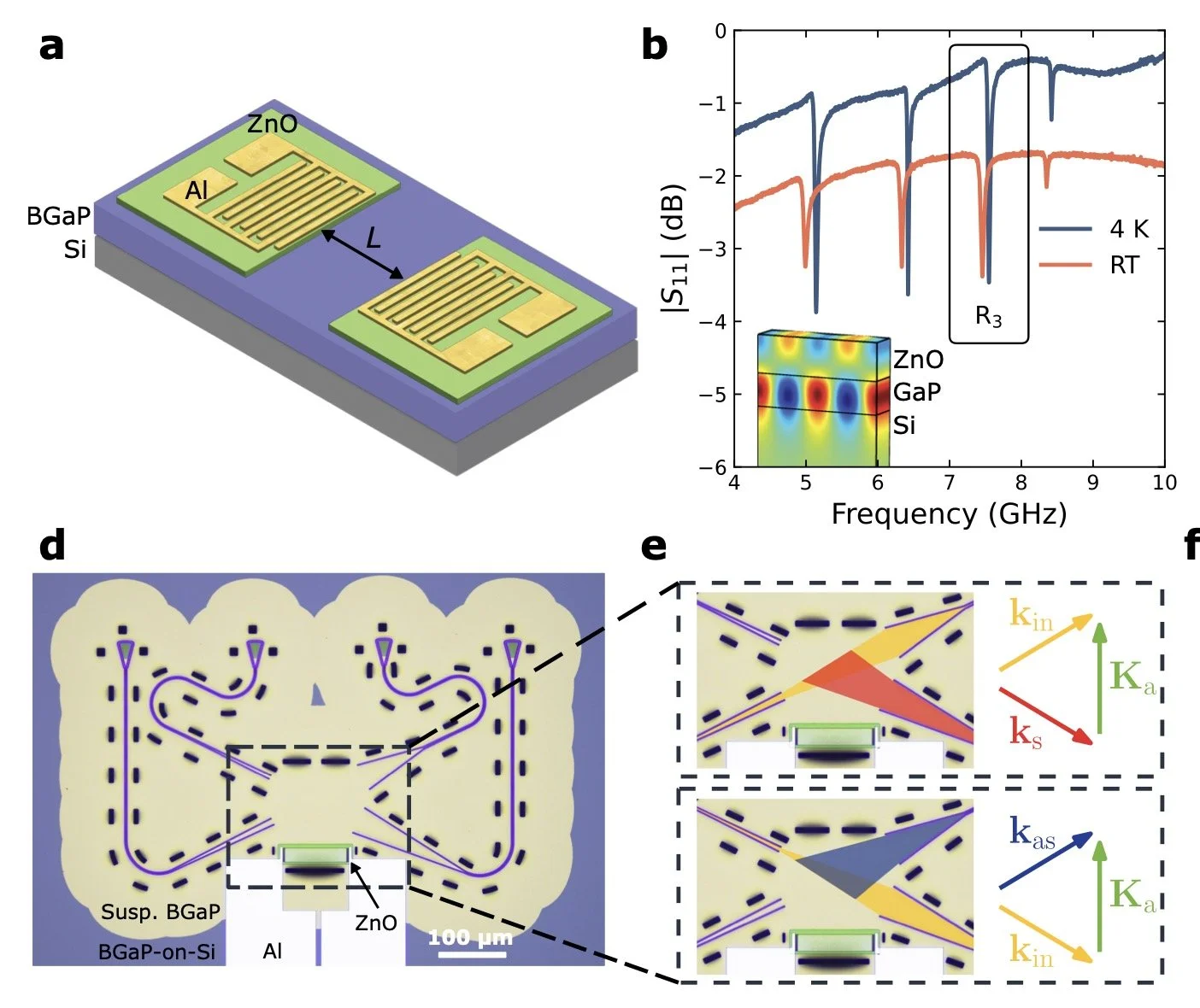
The compact size, scalability, and strongly confined fields in integrated photonic devices enable new functionalities in photonic networking and information processing, both classical and quantum. Gallium phosphide (GaP) is a promising material for active integrated photonics due to its high refractive index, wide band gap, strong nonlinear properties, and large acousto-optic figure of merit. In this work we demonstrate that silicon-lattice-matched boron-doped GaP (BGaP), grown at the 12-inch wafer scale, provides similar functionalities as GaP. BGaP optical resonators exhibit intrinsic quality factors exceeding 25,000 and 200,000 at visible and telecom wavelengths respectively. We further demonstrate the electromechanical generation of low-loss acoustic waves and an integrated acousto-optic (AO) modulator. High-resolution spatial and compositional mapping, combined with ab initio calculations indicate two candidates for the excess optical loss in the visible band: the silicon-GaP interface and boron dimers. These results demonstrate the promise of the BGaP material platform for the development of scalable AO technologies at telecom and provide potential pathways toward higher performance at shorter wavelengths.
To view the paper, click here.
